

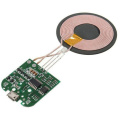

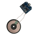
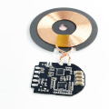
Wireless Charger PCBA Assembly PCB
| Unit Price: | 12 USD |
|---|---|
| Min. Order: | 1 Piece/Pieces |
| Transportation: | Ocean,Land,Air,Express,Others |
|---|---|
| Supply Ability: | 10000pcs/day |
| Port: | shenzhen |
Basic Info
Model No.: Aluminium Wireless Charger PCBA
Product Description
What is PCB made of?
PCB is composed of multiple layers of materials, each of which has a different purpose. They are laminated together by heating and adhesive to form a single object, a bit like lasagna.
Base material (FR4)
The substrate is usually glass fiber, and the most common type is "FR4". Such as Double-sided F4BM350 high frequency board. When using other base materials, many base materials lack the durability provided by FR4. The solid core provides rigidity and thickness to the PCB and insulation for other layers. For PCBs with lower rigidity, flexible high-temperature plastics (Kapton or equivalent materials) can be used as the basis to produce Flex High Quality PCB Products Flex.
copper
The next layer is thin copper foil. According to the requirements of custom pcb fabrication, copper can be applied to one or both sides of the substrate. The number of copper layers determines the type of board. Double-sided or double-sided boards have copper on both sides of the substrate, while single-sided boards have copper on only one side. In a typical PCB, you will find 0-18Layer FR4 board copper, of which 2 layers are the most common.
The copper layer provides conductivity to the PCB. Chemical etching divides the copper into multiple wires (called traces), connecting pads, and other functions that form the basis of the circuit on the PCB. These traces replace the wires used in the old version, and are insulated from each other by air and the substrate material.
Solder mask
Next is a layer of solder mask. The solder mask is usually green, but it can be any other color.
Solder resist is used to insulate copper traces to prevent accidental contact with other metals, solder, or conductive elements. The solder mask covers most of the area on the PCB, including small traces, but retains small loops and pads so that users can solder PCBA as needed.
Silk screen
Above the solder mask is the screen printing layer. This layer is purely for aesthetic purposes, adding letters, numbers and symbols to the PCB to make PCBA Manufacturing easier and easier for people to understand the board. Screen printing is usually used to indicate the function of each pin or LED. Screen printing is usually white, but any ink color can be used.


Product Categories : Aluminum Base Board > Aluminum LED Board